|
Shenzhen Tianweisheng Electronic Co., Ltd.
|
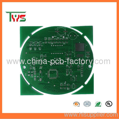
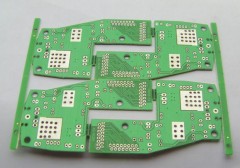
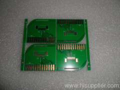
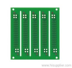
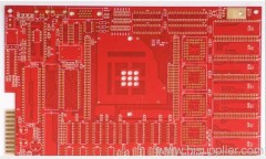
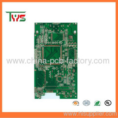
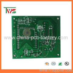
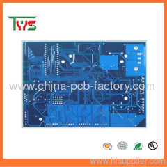
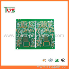
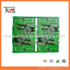
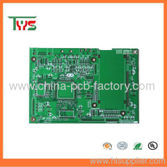
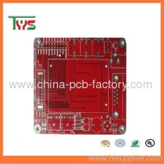
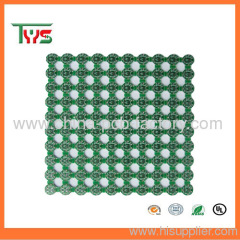
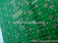
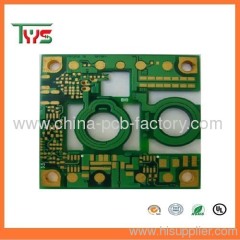
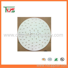
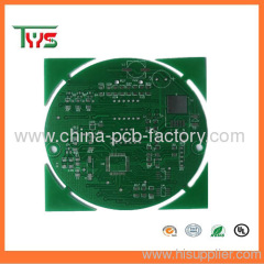
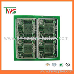
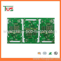
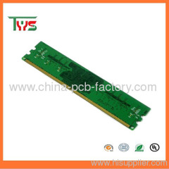
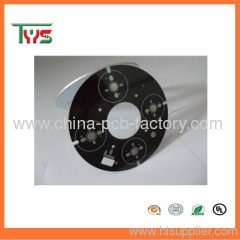
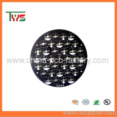
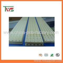
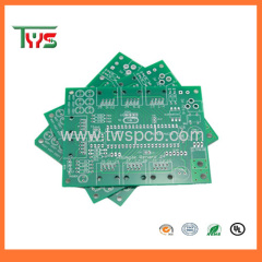
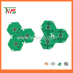
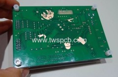
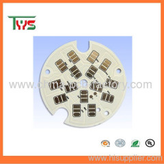
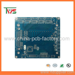
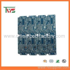
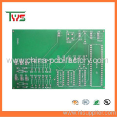
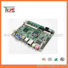
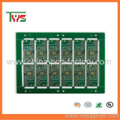
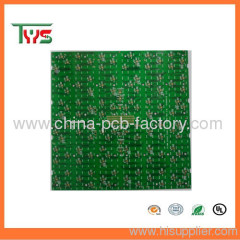
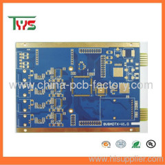
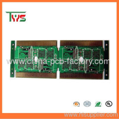
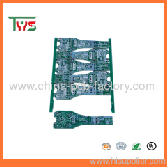
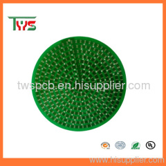
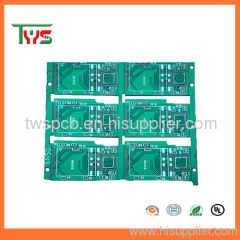
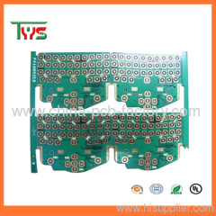
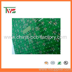
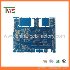
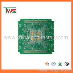
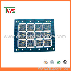
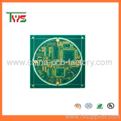
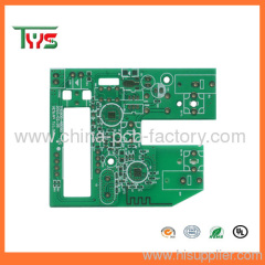
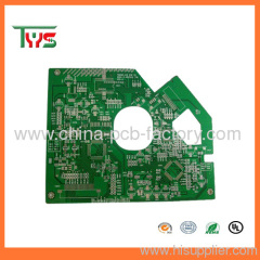
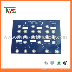
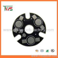
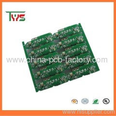
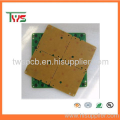
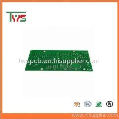
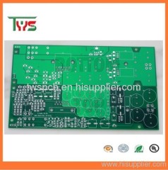
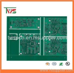
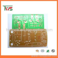
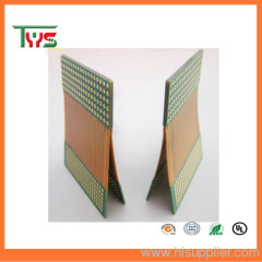
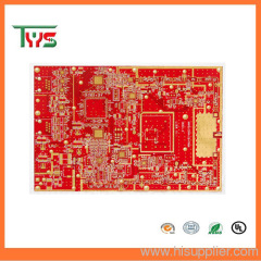
pcb board mobile designing
| Price: | 0.1~1.0 USD |
| Payment Terms: | T/T,WU;Paypal |
| Place of Origin: | Guangdong, China (Mainland) |
|
|
|
| Add to My Favorites | |
| HiSupplier Escrow |
Product Detail
pcb board mobile designing
1.15 year experience
2.Quickly Delivery
3.PCB Clone Copy
4.UL,ROHS,SGS.CE,ISO9001,TS16949
pcb board mobile designing
Contract Manufacturing

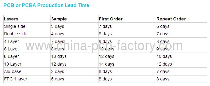
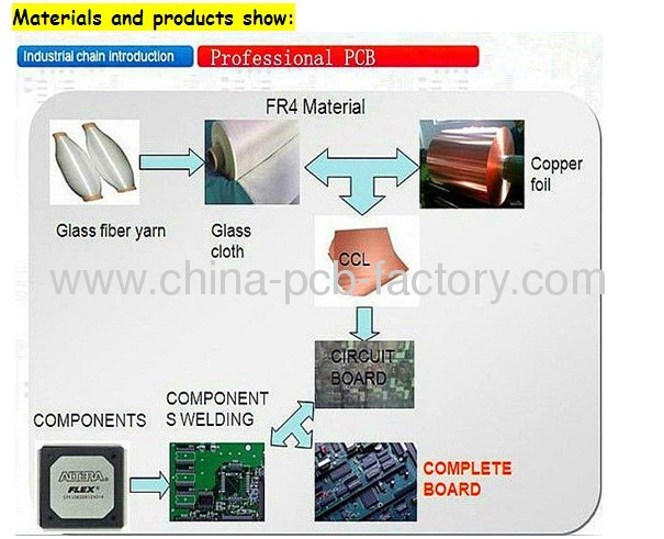
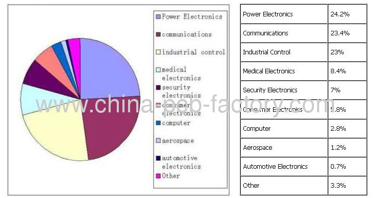


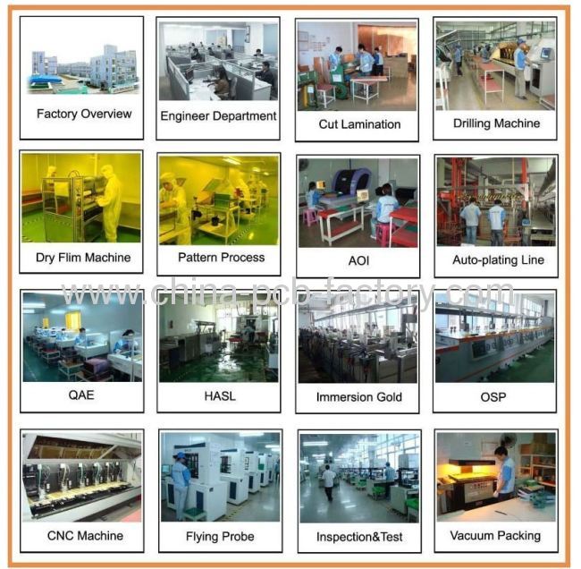
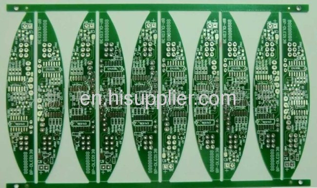
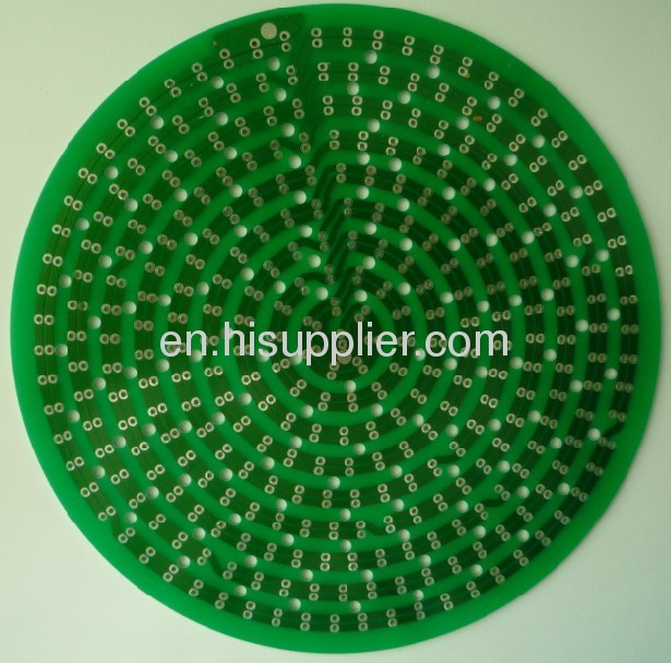
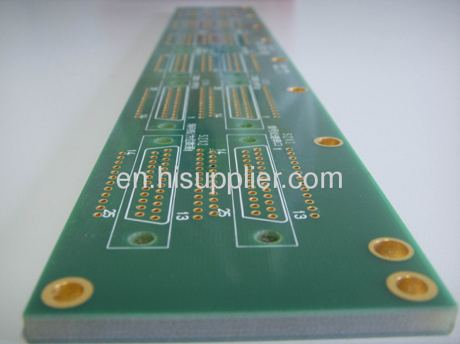
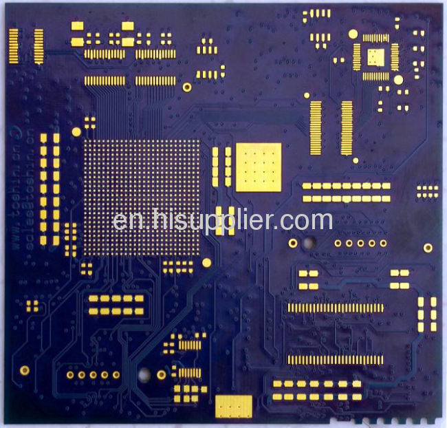
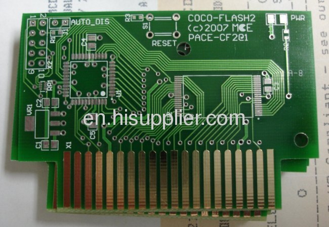
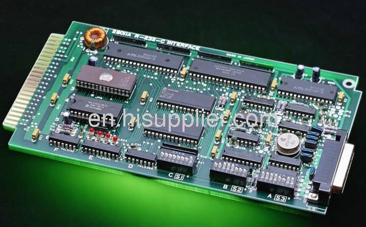
Contract Manufacturing
- Engineering Services
- PCB Design & Assembly
- Product Design
- Prototyping
- Cable and Wire Assemblies
- Plastics and Molds
Technical requirement:
Capacity of pcb
Technical requirement:
1) Professional Surface-mounting and Through-hole soldering Technology
2) Various sizes like 1206,0805,0603 components SMT technology
3) ICT(In Circuit Test),FCT(Functional Circuit Test) technology.
4) PCB Assembly With UL,CE,FCC,Rohs Approval
5) Nitrogen gas reflow soldering technology for SMT.
6) High Standard SMT&Solder Assembly Line
7) High density interconnected board placement technology capacity.
Quote requirement:
- Gerber file of the bare PCB board
- BOM (Bill of material) for assembly
- To short the lead time, please kindly advise us if there is any acceptable components substitution.
- Testing Guide & Test Fixtures if necessary
- Programming files & Programming tool if necessary
- Schematic if necessary
OEM/ODM/EMS Services for PCBA:
- PCBA, PCB assembly: SMT & PTH & BGA
- PCBA and enclosure design
- Components sourcing and purchasing
- Quick prototyping
- Plastic injection molding
- Metal sheet stamping
- Final assembly
- Test: AOI, In-Circuit Test (ICT), Functional Test (FCT)
- Custom clearance for material importing and product exporting
Orientronic PCB assembly Equipment:
- SMT Machine: SIEMENS SIPLACE D1/D2 / SIEMENS SIPLACE S20/F4
- Reflow Oven: FolunGwin FL-RX860
- Wave Soldering Machine: FolunGwin ADS300
- Automated Optical Inspection (AOI): Aleader ALD-H-350B
- Fully Automatic SMT Stencil Printer: FolunGwin Win-5
Capacity of pcb
NO | ITEM | Technical Data |
1 | Layer | 2-20 Layers |
2 | Board material | FR4,FR4 Halogen free,TEFLON Rogers,Getek High-TG(TG>170),Aluminium base |
3 | Max.Board Size0 | 457*660mm |
4 | Min.Board Thickness | 2 layers 0.2mm |
4 layers 0.4mm | ||
6 layers 0.8mm | ||
8 layers 1.0mm | ||
10 layers 1.2mm | ||
5 | Max.Board Thickness | 8.0mm |
6 | Min.Line Width | 0.05mm |
7 | Min.Line Space | 0.05mm |
8 | Min.Hole Size0 | Electroplating Via 0.15mm |
Micro via 0.075mm | ||
9 | PTH Wall Thickness) | 20-25um |
10 | Max.finish copper thickness0 | 8OZ |
11 | PTH Dia.Tolerance | ±0.05mm |
12 | NPTH Dia.Tolerance | ±0.025mm |
13 | Hole Position Deviation | ±0.05mm |
14 | Outline Tolerance | ±0.1mm |
15 | Min.S/M Pitch | 0.08mm |
16 | Insulation Resistance | 3x10Sec, 288°C |
17 | Warp and Twist | ≤0.7% |
18 | Electric Strength | >1.3KV/mm |
19 | Peel Strength | ≥1.4N/mm |
20 | Solder Mask Abrasion | ≥6H |
21 | Flammability | 94V0 |
22 | Impedance Control | ±5% |


PCB BOARD MOBILE DESIGNING
Didn't find what you're looking for?
Post Buying Lead or contact
HiSupplier Customer Service Center
for help!
Related Search
PCB Board
Pcb Mobile Phone
Rigid Pcb Board
Flex Pcb Board
Double Side Pcb Board
Pcb Smt Board
More>>

